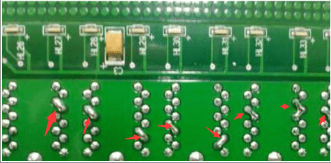
Cheap pcb manufacturing wave soldering analysis
date:Oct 17,2019
Return listCheap pcb manufacturing wave soldering analysis
The performancesof the solder joint qualification criteria aresas follows:

1.The surface of the wave solder joint should be complete, continuous and smooth, the amount of solder is moderate, no air holes, sand holes.
2. The wettability of the solder joint is good, and it is in the shape of a crescent moon. The wetting angle of the inserted component should be smaller than90°, preferably 15°-45°; the wetting angle of the chip component should also be smallerthan 90°. The solder should be spread out at the metallized end of the chip component to form a continuous uniform coating.
3. Defects such as solder leakage, virtual weldingand bridgingconnectionshould be minimized.
4. After soldering, the mounted components have no loss, and the terminal electrode does not fall off.
5. When soldering the doublesided pcb, it is required that the surface of the component of the component is in good tinned.
6. After soldering, the surface of the printed board is allowed to have slight discoloration, but no serious discoloration is allowed, and the solder mask is not allowed to foam and fall off.

