


HDI PCBs
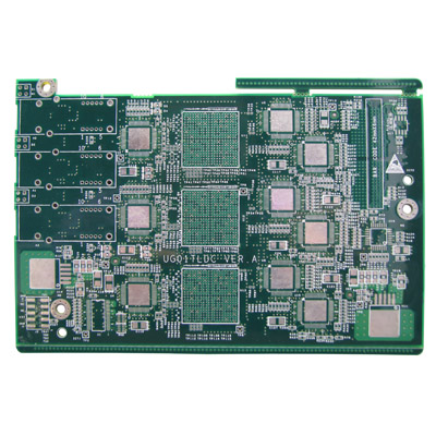
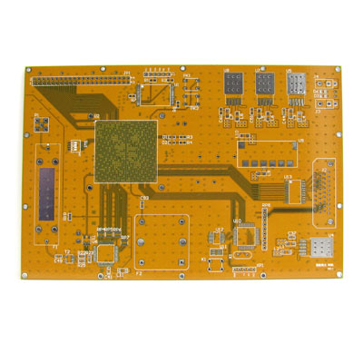
HDI Circuit Board
HDI is the abbreviation of High Density Interconnector. It is a (technology) for the production of printed circuit boards. It uses micro-blind and buried via technology for a circuit board with arelatively high line distribution density. HDI is a compact product designed for small-capacity users. It adopts modular design that can be connected in parallel. One module has a capacity of1000VA (1U height) and is naturally cooled. It can be directly placed in a 19" rack, and up to 6 modules can be connected in parallel. The product adopts full digital signal processing (DSP)technology and multiple Patented technology, with full range of adaptable load capacity and strong short-term overload capacity, regardless of load power factor and crest factor.
HDI Circuit Board Introduction
HDI circuit board (High Density Interconnector), that is, high-density interconnection board, is a circuit board with a relatively high line distribution density using micro-blind buried viatechnology. The HDI board has an inner layer circuit and an outer layer circuit, and then uses processes such as drilling and metallization in the hole to realize the internal connection of eachlayer of the circuit.
HDI circuit boards are generally manufactured by layer-by-layer method, and the more the number of layers, the higher the technical grade of the plate. Ordinary HDI boards are basically one-timebuild-up. High-end HDI uses two-time or more build-up technology. At the same time, advanced PCB technologies such as stacking holes, electroplating and filling holes, and laser direct drilling areused.
When the density of the PCB increases beyond the eight-layer board, it is manufactured with HDI, and its cost will be lower than that of the traditional and complex pressing process. HDI board isconducive to the use of advanced packaging technology, and its electrical performance and signal accuracy are higher than traditional PCB. In addition, HDI boards have better improvements in radiofrequency interference, electromagnetic wave interference, electrostatic discharge, and heat conduction.
HDI Circuit Board Application
While electronic design continues to improve the performance of the whole machine, it is also working hard to reduce its size. In small portable products ranging from mobile phones to smartweapons, "small" is an eternal pursuit. High-density integration (HDI) technology can make terminal product designs more compact, while meeting higher standards of electronic performance andefficiency.
HDI is widely used in mobile phones, digital (camcorder) cameras, MP3, MP4, notebook computers, automotive electronics and other digital products, among which mobile phones are the most widelyused. HDI boards are generally manufactured by the build-up method. The more build-up times, the higher the technical grade of the board. Ordinary HDI boards are basically one-time build-up. High-end HDI uses two-time or more build-up technology. At the same time, advanced PCB technologies such as stacking holes, electroplating and filling holes, and laser direct drilling are used. High-endHDI boards are mainly used in 3G mobile phones, advanced digital cameras, IC carrier boards, etc.
HDI Circuit Board Advantages
1. It can reduce the cost of PCB: When the density of PCB increases to more than eight-layer board, it is manufactured by HDI, and its cost will be lower than that of the traditional and complexpressing process.
2. Increase circuit density: the interconnection of traditional circuit boards and parts
3. Conducive to the use of advanced construction technology
4. Have better electrical performance and signal accuracy
5. Better reliability
6. Can improve thermal properties
7. It can improve radio frequency interference/electromagnetic wave interference/electrostatic discharge (RFI/EMI/ESD)
8. Increase design efficiency