PCB Layout design flow
date:Nov 05,2018
Return listPCB Layout design flow

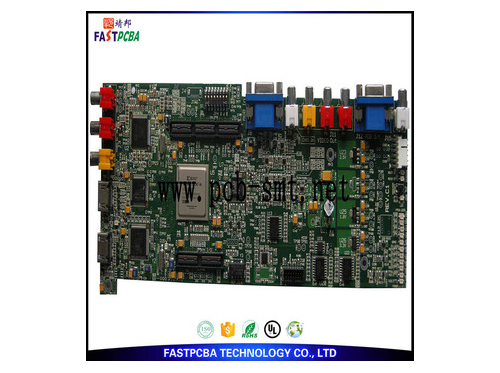
To complete a PCB board, it can be basically divided into three main stages, the first stage circuit diagram drawing, the second stage circuit layout, and the third stage is to build a BOM table, and then prepare materials for hand and hand soldering.
If your PCB needs to be laid out above 4 layers or high speed, RF, antenna such as high frequency, this is already pro professional level, it is not easy without expert guidance, plus you don't have too many measuring instruments. Some are also unlikely to do it themselves. This is another level. It is recommended to find a Layout House OEM with relevant design expertise, because there may be EMI, FCC, CE, and NCC specifications.
Recommend
-
24Nov
Comparison of leaded and lead-free processes for PCBA processing
-
04Nov
PCB manufacturing reflow soldering furnace technical indicators and development direction
-
21Nov
What are the benefits of using fpc boards?
-
06Nov
PCB manufacturing solder joint strength and connection reliability analysis

